Background
Research in our lab focuses on the development of novel functionalities driven by spin and quantum effects in oxide thin films. Materials with “designer interfaces” are investigated to discover new paradigms for quantum materials and low-energy next-generation sensors and actuators; in doing so we realize disruptive nanoelectronics technologies beyond convention silicon CMOS. The successful outcomes achieved have a significant impact on future devices in terms of energy efficiency, operating speed, and manufacturing reliability.
Big picture significance: Why should you care?
Energy creation and consumption are two of the defining challenges of the 21st century. Significant emphasis is already being placed on the creation aspect; however, it is consumption demands and patterns that often shape the materials development landscape. Our research focuses on the consumption aspect. Our research goals address three of the grand challenges identified by the U.S. Department of Energy, the UK Engineering and Physical Sciences Research Council, and the US National Academy of Science:
(1) How will the energy demands of future generations be met?
(2) What new discoveries await us in the nanoworld?
(3) How will the information technology revolution be extended?
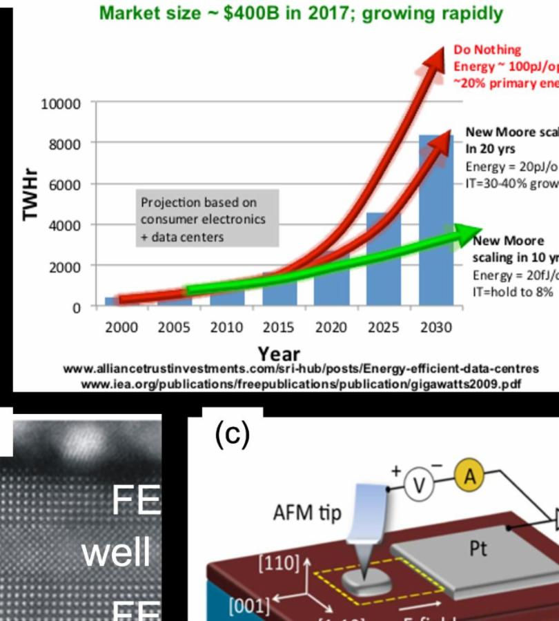
Our society relies on the cheap availability of energy, ideally generated without destroying our planet. Once energy is generated, we primarily use it for manufacturing, transportation, and increasingly for information and communications technologies. While the energy demands of the first two sectors have remained relatively static, IT and communications currently consume approximately 5% of the world’s electrical power and demand is increasing [see Fig. 1(a)]. Your smart phone and the data center that supports it already consume more power than your refrigerator! Future growth in information technology (IT), and the advent of the “internet-of-things” mean that if current rate of increase is unchecked, consumption in this sector will climb to almost 20% of the primary energy produced.
The grand challenge our research program addresses is the development of new materials and technologies to increase the efficiency of energy consumption in IT sectors.
At the quantum level, electronic, photonic, vibrational or plasmon (even forbidden) properties can exist uniquely. These quantum properties open significant new degrees of freedom in the design of functional materials systems [1]. Consequently, they enable new logic devices and memories that require a fraction of the power of traditional electronics. This opens innovative ways for functional control at unprecedented efficiencies, thereby revolutionizing energy consumption [2,3].
The research project:
This thesis will develop quantum materials that can form the basis of new device structures [e.g., Figure 1(b,c)] for low energy computation [4]. The student will design, fabricate, and characterize oxide thin film heterostructures and tunnel junction devices for integration with spintronics. The student should have previous experimental experience with materials science and/or physics, and a desired understanding of crystallography.
Supervisors
Supervisor: Daniel Sando
Key qualifications and skills
The student should have previous experimental experience with materials science and/or physics, and a desired understanding of crystallography.
Does the project come with funding
Yes - 28k NZD (topup possible) for 3 years
Final date for receiving applications
Ongoing
Keywords
oxide thin films, spintronics, multiferroics, materials, physics


